Design Services
Substrate Design
- Ceramic or Laminates
- Single or Multiple Layers
- Thick or Thin Film
- Single or Multiple Chips
- Peripherals, Leads, or Ball Grid Arrays
Lead Frame Design
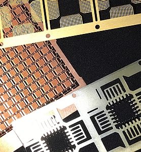
- Clip Lead Frame or Flat Leads
- Solder Laden or Solderless Clip Head
- Continuous Strip, Stamped or Etched Strips, & Quads
- Single in Line, Dual in Line, and Quad Flat Packs
- 0.4mm, 0.5mm, 0.65mm, 0.025″, 0.050″, 0.100″ Pitch
Package Design
The package serves several competing functions to the electronics such as, integrating components, interfacing components to the overall circuit or system, provide protection from environment, support mechanically and provide thermal path for heat sink. Package design and material selection to fabricate the package play a very critical role in the reliability and performance of the device.
FLI offers a broad range of standard and application specific microelectronics packaging schemes. We have designed and packaged devices for medical, automotive, power, sensors, telecommunications, control and defense industries for more than 15 years.
Our packaging services cover modules for optoelectronic communications, multichip modules for MEMS and sensors, high speed radio frequency and microwave packages, transistor outline packages, Kovar packages, dual in line, hermetic power packages, flip chip package for power devices, telecom packages, hybrid packages, and chip on boards.
FLI’s engineers have the experience and creativity to deliver the most reliable and manufacturable packaging services at a low cost and in a timely manner.
Our package design service offers design-to-prototype:
- Package design and layout
- New package development and prototype
- Process development and characterizations
- Consultations on various packaging techniques and technologies
- Technology transfer for mass production